Major Title to R-Type (M72) Conversions
The conversions use a modified version of the M72-based game code created by Chris Hardy using his R-Type emulator.
Please note that these ROM image sets are not suitable for use with any emulator.
What you need
In addition to the 4 x 27C010 and 1 x 27512 already on Major Title that can be re-used, you will need the following items:-
- A modified ROM image set for the game:-
| R-Type |
RTYPEMT.ZIP |
| other games |
T.B.A. |
- 4 x 27C020 or equivalent
- 5 x 27C010 or equivalent
- 9 x 32-way DIL sockets
- 1 x 28-way DIL socket
- 1 x HM62256-12 or equivalent.
- 1 x 74LS244
- 1 x 74LS32
- A length of wire-wrap wire.
Mask ROM Removals
The following ROMS need to be removed and 32-pin sockets need to be fitted in their place where applicable.
CPU Board
IC12
IC15
IC48 (C1)
IC49 (C0)
IC56 (C3)
IC57 (C2)
Video Board
IC36 (N3)
IC44 (N0)
IC45 (N1)
IC46 (N2)
Replacement EPROMS
Blank all the EPROMS and program in the hacked images according to the list below:-
CPU Board
*_V0 into 27C010 for location IC12 (not used on R-Type)
*_SP into 27C512 for location IC15
*_C1 into 27C020 for location IC48 (C1)
*_C0 into 27C020 for location IC49 (C0)
*_H1 into 27C010 for location IC51
*_H0 into 27C010 for location IC52
*_C3 into 27C020 for location IC56 (C3)
*_C2 into 27C020 for location IC57 (C2)
*_L1 into 27C010 for location IC59
*_L0 into 27C010 for location IC60
Video Board
*_N3 into 27C010 for location IC36 (N3)
*_N0 into 27C010 for location IC44 (N0)
*_N1 into 27C010 for location IC45 (N1)
*_N2 into 27C010 for location IC46 (N2)
Jumper Changes
There are few jumpers that need to be changed to reflect the EPROM memory configuration.
CPU Board
J2 (opposite IC12 pin 31) from "MASK" [--O] to " EP " [O--]
J4 (opposite IC48 pin 30) from " OT " [O--] to " 2M " [--O]
J5 (opposite IC48 pin 25) from "1MM " [O--] to " OT " [--O]
Hardware Modifications - CPU Board
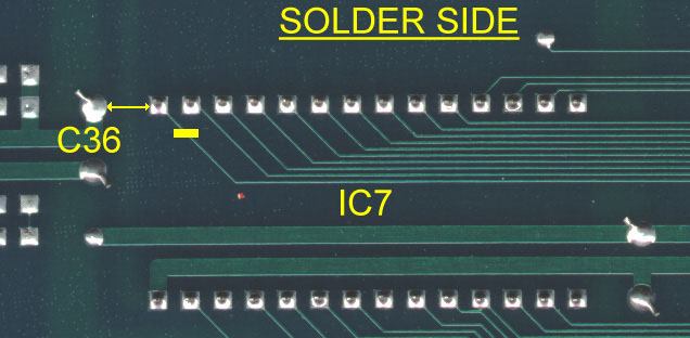
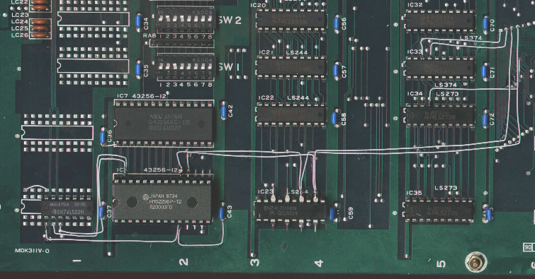
Locate IC7 (43256-12). Cut the track leading from pad 1 on the solder side of the board.
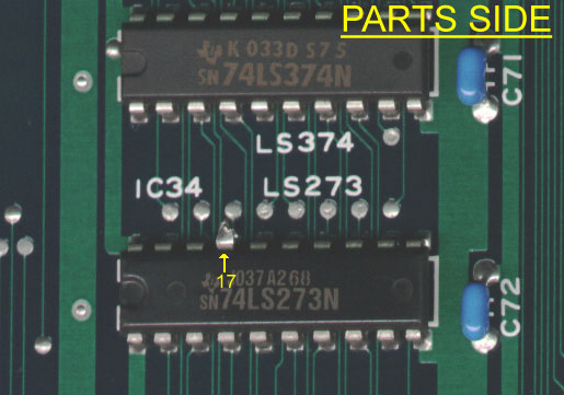
Locate IC34 (LS273). Cut and lift pin 17 such that the pin is no longer connected to the PCB pad.
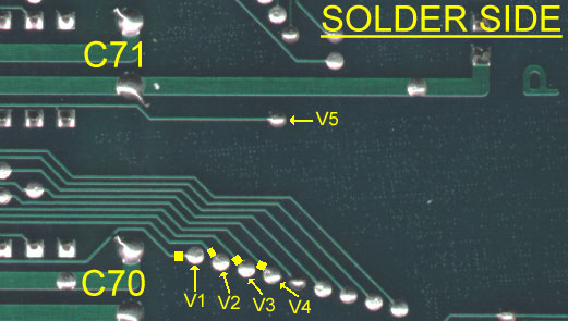
Locate capacitor C70 (next to IC32). Just below C70 is a diagonal row of 9 vias. On the solder side of the PCB cut the tracks leading from the first four vias down from C70. For reference these vias will be called V1 to V4. The via located 12mm directly to the right of V4 will be called V5.
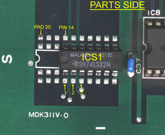
Fit the 74LS32 into the bottom of the spare site just above IC8. Only pins 1,2,3,7 and 14 need to be soldered. For reference this will be ICS1 and will be referred to as a 14-pin device fitted to a 20-pad site. The pins for the spare locations are brought out to pads adjacent and these can be used for pin connections.
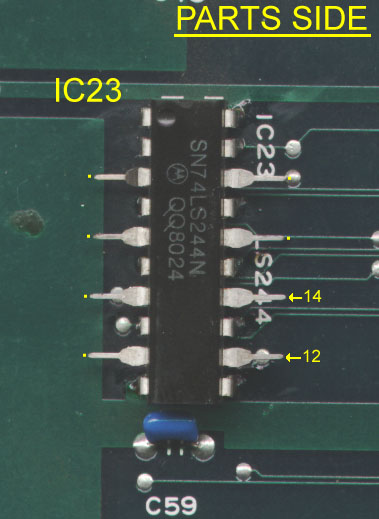
Locate IC23 (LS244). Fit the 74LS244 on top of IC23 with pins 3,5,7,9,12,14,16 and 18 lifted and the rest soldered to the pins on IC23. For reference this will be IC23(T) and the original device underneath will be IC23(B).
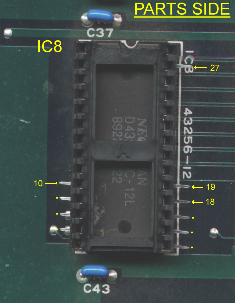
Locate IC8 (43256-12). Fit the 28-way socket on top of IC8 with pins 10,11,12,13,15,16,17,18,19 and 27 lifted and the rest soldered to the pins on IC8. For reference this will be IC8(T) and the original device underneath will be IC8(B).
Use the wire-wrap wire to make the following connections:-
| IC7 pin 1 |
-> |
C36 GND |
|
|
(len. 6mm exc. bare ends) |
| IC8(T) pin 10 |
-> |
C43 GND |
|
|
(len. 27mm exc. bare ends) |
| IC34 pin 17 |
-> |
via V5 |
|
|
(len. 50mm exc. bare ends) |
| IC8(T) pin 18 |
-> |
IC23(T) pin 14 |
-> |
via V4 |
(len. 63mm & 135mm exc. bare ends) |
| IC8(T) pin 19 |
-> |
IC23(T) pin 12 |
-> |
via V3 |
(len. 72mm & 130mm exc. bare ends) |
| IC33 pin 17 |
-> |
via V2 |
|
|
(len. 38mm exc. bare ends) |
| IC33 pin 18 |
-> |
via V1 |
|
|
(len. 38mm exc. bare ends) |
| ICS1 pin 1 |
-> |
IC8(B) pin 10 |
|
|
(len. 60mm exc. bare ends) |
| ICS1 pin 2 |
-> |
IC8(B) pin 27 |
|
|
(len. 66mm exc. bare ends) |
| ICS1 pin 3 |
-> |
IC8(T) pin 27 |
|
|
(len. 60mm exc. bare ends) |
| ICS1 pin 14 |
-> |
ICS1 pad 20 (+5V) |
|
|
(len. 8mm exc. bare ends) |
Finally, insert the HM62256-12 into the socket of IC8(T) to complete the conversion.
Modified M72 Game Images
| Game |
File Name |
Size |
Date |
| R-Type |
RTYPEMT.ZIP |
823,991 |
07/07/2009 |